विशेष लेख
Eight Intriguing Insights Into the World of Semiconductors
Every electronic instrument we use today is integrated with semiconductors. Behind the functionality of our vehicles, mobile devices, computers, and intelligent home systems lies a complex arrangement of microscopic parts, each performing a distinct role to ensure the device operates correctly. While they are foundational to modern life, the specific mechanics of these tiny components often go unnoticed. This article explores several key details about the technology that powers our daily routines.
Victoria Anne Kingsley
लेखक
लेख परिचय
नीचे पूरा लेख पढ़ें।
अनुभाग
समाचार
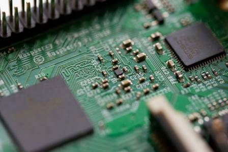
Every electronic instrument we use today is integrated with semiconductors. Behind the functionality of our vehicles, mobile devices, computers, and intelligent home systems lies a complex arrangement of microscopic parts, each performing a distinct role to ensure the device operates correctly. While they are foundational to modern life, the specific mechanics of these tiny components often go unnoticed. This article explores several key details about the technology that powers our daily routines.
The Physical Composition and Nature of Semiconductors
Semiconductors are manufactured using materials that possess a unique level of electrical conductivity. Their ability to move electricity falls between that of metals, which are excellent conductors, and insulators, which are highly resistant to electrical flow. A critical feature of these materials is that their conductivity can be precisely managed by introducing small quantities of other elements. Because of this sensitivity, manufacturers must take extreme care regarding moisture levels, electrical overstress, and static discharge during the production process.
The Complexity and Density of Modern Microchips
A microchip is a sophisticated structure containing millions, or even billions, of transistors and various other electronic parts. These components are interconnected by multiple layers of intricate circuitry. Over the decades, the ability to integrate smaller parts into a single package has made processors increasingly robust. This progression follows a famous industry observation known as Moore’s Law, which suggests that the density of transistors on an integrated circuit roughly doubles every twenty-four months.
High-Tech Manufacturing in Specialized Environments
The facilities where these components are made are known as "fabs," short for semiconductor fabrication plants. Inside these buildings are "clean rooms"—highly controlled spaces where air quality, temperature, and humidity are strictly regulated. Such precision is necessary because even a single microscopic particle of dust can ruin the delicate circuitry of a chip during production.
The Intensive Production Process of Silicon Wafers
The journey of a chip begins with a wafer, which is a thin, highly purified slice of silicon. This wafer acts as the foundation for the finished product. To create the necessary electronic patterns, the material undergoes an exhaustive series of treatments, including cleaning, stripping, and chemical etching. This rigorous procedure can involve 500 or more individual steps to ensure the final substrate is perfect.
Global Distribution and Massive Market Scale
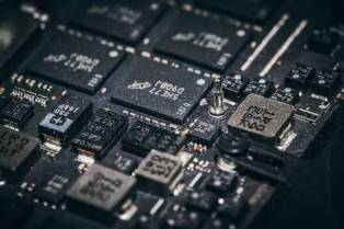
The scale of the semiconductor industry is immense. In a single year, global sales reached nearly 1.14 trillion units. This equates to approximately 140 chips for every individual on Earth, or a production rate of 130 million units per hour. To visualize this volume, if all these semiconductors were stacked vertically, the pile would reach far beyond the heights at which commercial jets fly.
The Evolution of Materials in Chip Design
As technology has advanced, the variety of chemical elements used in manufacturing has expanded significantly. Early versions of these devices relied on germanium, but the industry shifted quickly to silicon due to its superior properties. Researchers are currently investigating a wider range of elements and new chemical compounds to find materials that can support future applications and even more powerful computing needs.
Primary Categories of Integrated Circuits
Microchips are generally categorized into two main types: logic and memory. Logic chips act as the "brain" of a device, performing the calculations and processing tasks required to run software on a smartphone or computer. Memory chips, on the other hand, are designed for storage. This includes DRAM for temporary data handling while a device is active, as well as long-term storage solutions like hard drives.
The Incredible Precision of Microscopic Architecture
The features found on the most sophisticated chips today are incredibly small, with some measured at just 7nm. For perspective, a single strand of human hair is nearly 10,000 times wider than these microscopic structures. This level of precision allows for the extreme density and high performance found in modern consumer electronics.
यह भी पढ़ें

वास्तविक जैसी तस्वीरें पेंट करने की विधि
आदित्येश

Smart Casual for Men: The Definitive 2025 Style Guide
Jacob

2025 में दुनिया की शीर्ष 10 सबसे तेज़ कारें
राधा

क्या माउंट एवरेस्ट पर चढ़ना आपको खुश करेगा? या क्या "शोर" आपके रास्ते में आएगा?
सरिता

स्टिल लाइफ पेंटिंग की कला में महारत हासिल करें: नौ चरणों वाली निर्देशात्मक मार्गदर्शिका
नीलांजन दास

सिंगापुर को एक नए नजरिए से देखने के लिए 6 सर्वश्रेष्ठ टूर
लता